| << PARTS LISTING |
![]()
If you have experience with PCB etching kits, I recommend to you that you use this other
![]() layout (Word
6 format) where you will find the circuit layout (7x3 cm.) Thanks to
kike for the excellent document.
layout (Word
6 format) where you will find the circuit layout (7x3 cm.) Thanks to
kike for the excellent document.
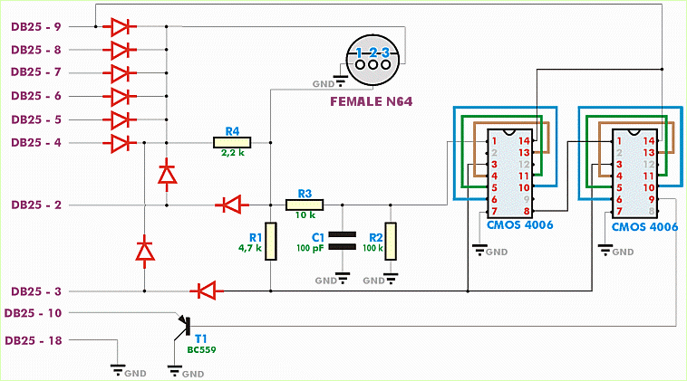
Schematic of the circuit
If you want to print a high-quality version of the schematics, get this .WMF
![]() Circuit in
WMF format (Windows metafile)
Circuit in
WMF format (Windows metafile)
As you can see, the circuit is a bit more complicated than the PlayStation one. If you pay attention, the connections to the chips (4006) leave and then return to enter the same chip. They are of different colors simply to make it easier to see the individual lines. They do not mean anything else. Both chips have the same configuration of connections that leave and return to enter.
Please use maximum care when putting the transistor (T1) and the chips into circuit, since if you are mistaken, you may fry them.
Aside from this, the greater complication of the circuit resides in being a little patient(?) to be able to make the connections under the experimental board. And following with my intention of making this as easy as possible, I drew out the graphical way or how I mounted the components, in case you need the guidance:
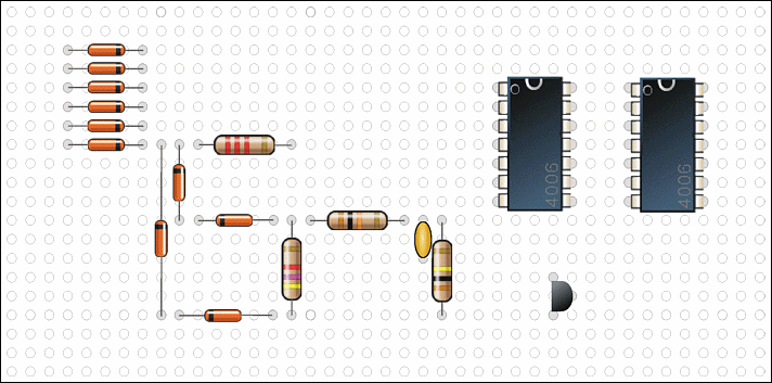
Assembly of the components on the prototype board
The connections will be made on the underside. I recommend that you cut off a 6 inch piece of the 10 conductor cable so you will have wire to make the connections on the underside of the board when the component leads aren't long enough.
And now we see the connections, looking up from the under-side of the board. Take into account that this view is not the same one that the one of above, it is horizontal mirror supposing that the circuit board is transparent (I know, nobody has X-ray vision to see it in reality).
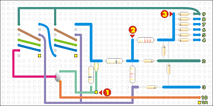
View of under-side of proto-board (with top side visible for reference)
The purpose of the different colors in the drawing is, like always, to avoid confusion. Now, I'll explain some other things to you.
The green numbers on the right are the points where the 10 wires
will connect to the pins on the DB-25. Solder in each one of the wires to
the circuit board, then solder the other end on the male DB-25 connector
as it corresponds to the drawing (according to the green number). 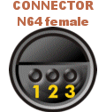
This symbol, ![]() ,
corresponds to the ground. You should solder a wire in each one of these points and
to take them all to the point where we will solder the wire corresponding to pin 18 of the DB-25.
,
corresponds to the ground. You should solder a wire in each one of these points and
to take them all to the point where we will solder the wire corresponding to pin 18 of the DB-25.
The yellow numbers in red circles correspond to the female connector of the Nintendo 64 controller. To the right is a picture of the female connector.